

Custom PCBA Design Services for IoT Hardware
Design, review, prototype, and validate connected hardware boards with firmware, radio, power, manufacturing, compliance, and field-service constraints in mind.
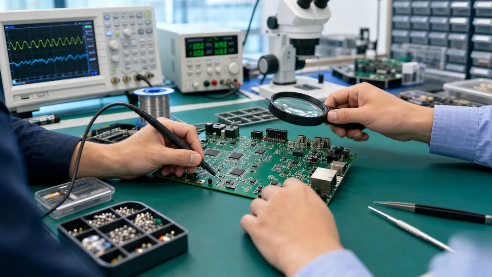
Schematic, layout, connectors, power, IO, RF, and manufacturability reviewed together.
Bring-up, firmware interface, test points, calibration, and failure records before production.
BOM risk, test fixtures, flashing, QA records, and maintenance notes prepared for handoff.
Design review, prototype bring-up, and field-fit validation belong in one loop
For connected hardware, the board is only one layer. The package also needs firmware touchpoints, gateway or cloud onboarding, enclosure fit, test points, and clear production evidence.

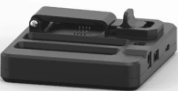
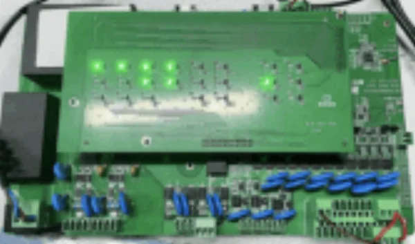
Power, radio, connectors, IO, supply risk, and test points are reviewed before sample build.
Firmware interface, flashing, calibration, measurement, and logs are checked on real boards.
Fixture needs, QA records, known limits, and service diagnostics are prepared for the next run.

PCBA design must fit the product workflow, not only the schematic
Connected hardware quality depends on how the board supports firmware, wireless behavior, enclosure constraints, factory testing, and future service operations.
- Review schematic, layout, BOM, and firmware interface together
- Plan test points, calibration, flashing, and QA records early
- Document known production risks before volume decisions
Workstreams that move the project toward a usable product
Each workstream connects a real device, workflow, user role, or operating constraint with the software and hardware decisions required for delivery.
Customized PCB design and layout
Board architecture, schematic, layout coordination, connector planning, IO, power, and radio constraints.
Existing product modification
Add sensors, wireless modules, edge compute, controller interfaces, or test access to mature products.
Full-cycle hardware development
From requirement review to prototype, firmware integration, test, and production handoff.
Embedded electronics design
MCU, wireless module, sensor, relay, display, storage, and peripheral decisions tied to firmware needs.
Electronics prototyping
Bring-up support, sample validation, measurement, failure records, and iteration recommendations.
FPGA or special module support
Plan advanced compute, signal, timing, or interface modules when the product requires it.
From board design to production-ready smart hardware
The design path keeps electrical, firmware, mechanical, manufacturing, and service requirements aligned.
Requirement and constraints
Target environment, interfaces, power, enclosure, wireless, sensor, and certification assumptions.
Schematic and layout
Component choices, circuit design, PCB layout, connectors, test points, and BOM decisions.
Prototype and firmware fit
Bring-up, drivers, flashing, calibration, payloads, and device identity prepared for software.
Validation and handoff
Functional testing, QA notes, fixture plan, production risks, and iteration recommendations.
Key engineering decisions to make before production
The most valuable work is often the integration boundary, recovery behavior, diagnostics, and ownership model that keeps the system maintainable.
Power and thermal design
Duty cycle, input range, heat, battery or adapter needs, and enclosure effects are reviewed.
Wireless and antenna fit
Wi-Fi, Bluetooth, 4G, LoRa, or gateway radio choices are checked against the installation environment.
Firmware interface contract
Pin mapping, boot mode, flashing, logs, calibration, and device-state fields are coordinated with firmware.
BOM and supply risk
Component lifecycle, cost, availability, alternates, and manufacturing assumptions are documented.
Factory test path
Test points, fixtures, serial numbers, flashing, calibration, and QA records are planned before production.
Compliance awareness
Safety, EMC, radio, enclosure, and market requirements are considered during architecture decisions.
A strong PCBA package reduces firmware, factory, and field risk
The board should be easy to bring up, test, flash, diagnose, and manufacture. That requires decisions beyond circuit drawings.
Key components and alternates are reviewed before production pressure.
Wireless choices are tested against enclosure and site conditions.
Production and service checks are included in the design path.

Where this service creates measurable product value
Service pages should show the operating environment, not only describe the technology stack.
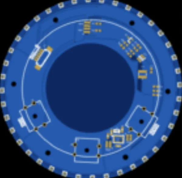
Smart equipment controllers
Custom boards for controllers, sensors, relays, alarms, and connected equipment upgrades.
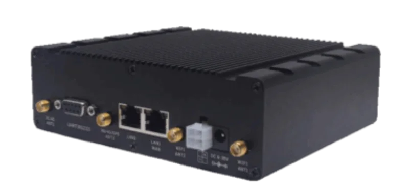
Industrial gateway hardware
Serial ports, Ethernet, 4G, power, IO, enclosure, and gateway board choices for field sites.
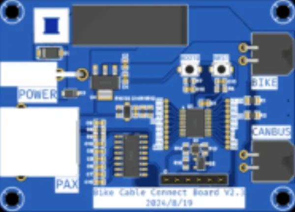
Sensor and monitoring devices
Low-power sensing, wireless modules, data acquisition, calibration, and production testing for IoT products.
What ZedIoT delivers
The output should help your team make a clear build decision, validate the first release, and keep the system maintainable after launch.
Design package
Requirement notes, schematic/layout review, BOM decisions, module choices, and design constraints.
Prototype validation
Bring-up records, measurements, firmware interface notes, test commands, and issue list.
Production handoff
Fixture needs, QA records, flashing process, calibration steps, and known risk notes.
How the work moves from feasibility to handoff
Requirements analysis
Confirm product scenario, interfaces, power, wireless, enclosure, compliance, and production assumptions.
Schematic and PCB design
Design or review circuit, layout, BOM, module selection, and test points.
Prototype production
Coordinate sample build, bring-up, firmware fit, and measurement records.
Testing and validation
Validate function, radio, power, temperature, firmware behavior, and production checks.
Continuous maintenance
Support iteration, component changes, firmware updates, and production feedback.
Practical advantages for AI + IoT product delivery
Hardware and firmware aligned
Board decisions are reviewed with firmware, cloud onboarding, diagnostics, and service workflows.
Production-minded validation
The work includes testability, flashing, calibration, QA records, and handoff details.
AI + IoT product context
We can connect board work to gateways, sensors, edge devices, apps, and platform operations.
Questions to resolve before scope is locked
Can ZedIoT design a complete PCBA from scratch?
We can support design, review, module selection, interface planning, prototype validation, and handoff. The exact scope depends on product maturity, certification needs, and manufacturing partner responsibilities.
How does firmware affect PCBA design?
Firmware requirements affect pin mapping, peripherals, storage, boot mode, test points, flashing method, calibration, wireless behavior, and how the device reports status to the platform.
Do you support BOM and production test planning?
Yes. BOM risk review, component availability, programming steps, test commands, calibration checks, and factory records can be included in the delivery scope.
Discuss PCBA Design Services
Share the device, workflow, system integration, deployment requirement, or business outcome you want to validate. We will help turn it into a practical AI + IoT implementation path.
- AI + IoT product architecture review
- Hardware, firmware, cloud, and application integration
- Prototype planning and production support