

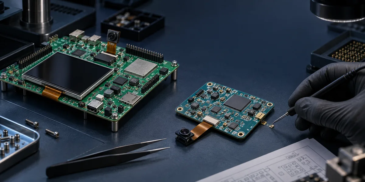
A screen, camera and network demo may all work on the ESP32-P4 Function EV Board. That is useful evidence for the particular board, components and firmware in front of you. It is not evidence that a new enclosure, flexible cable, power supply or PCB stack-up will behave the same way. Moving from the EV Board to a custom product therefore means transferring a set of design constraints, not copying a schematic and calling it qualified. The decisions most likely to escape an early review are chip revision, power domains, external Flash and in-package PSRAM, the complete MIPI path, the wireless companion, and whether either chip can still be programmed after a failure. See the official EV Board guide and P4 hardware design guide.
What a working development board does—and does not—prove
If the development board lights a display, its driver initialization sequence and interface choice are reasonable starting points. They do not qualify the new power rail, longer FPC or display stability in a different enclosure. A working camera does not validate another sensor's clock, control voltage, MIPI layout or mechanical assembly. Networking is a separate chain: Function EV Board v1.5.2 includes an ESP32-C6-MINI-1, but moving that module or substituting a C6/C5 design changes the RF environment, inter-chip wiring and firmware pairing. The board user guide identifies the reference configuration; it cannot qualify your replacement.
At project kickoff, create a three-column register: reference-board condition, product-board change, and evidence needed to accept that change. Record the EV Board hardware version, actual P4 silicon revision, display and sensor part numbers, FPC, P4/C6 firmware revisions and external Flash. Without that baseline, every bring-up problem can be blamed on either “hardware” or “software” without a useful way to separate them.
| What the EV Board provides | What the product board must decide | Evidence to retain |
|---|---|---|
| P4 reference circuit | Silicon revision, package, power and reset network | Purchased part number, errata comparison, schematic review |
| Camera/display demos | Actual sensor and panel, connectors, FPC, control voltages and lanes | Component documents, pin and voltage map, layout review, target-board observations |
| C6 networking example | Companion module, antenna position, P4–C6 wiring and reset | Both firmware identities, handshake logs, RF test plan |
| USB/UART debug path | Accessible production test points, programming jig and recovery route | Flash and failed-update recovery records |
The last column lists deliverables, not measurements that this article has performed. Public documentation cannot populate the “passed” field for an unknown PCB.

“Target-board test records” is a required future evidence step in this diagram, not a test result supplied here.
Make each change traceable to a part number
Version the delta list for connectors, sensors, panels, wireless modules, Flash and power components. Each row should show the old board and part revision, replacement candidate, changed voltage or signal, relevant official requirement, owner and pending test. Even an unchanged component needs an explicit revision: purchasing substitutions and firmware updates can otherwise make two nominally identical boards materially different.
Keep design inputs separate from test outcomes. Before layout you can specify lane count, voltage, resolution, expected peak current and available enclosure space. Only after target-board bring-up can you record power waveforms, MIPI errors, lost frames, wireless recovery or hot-condition behavior. A planned test is not a passed test. Have the hardware lead sign off design inputs, the firmware lead sign off drivers and log points, and the test lead record actual sample results.
Freeze silicon revision and power before choosing peripherals
Espressif's P4 guidelines distinguish silicon revisions. Some pin definitions and reference circuits differ between newer v3.0-and-later devices and older v1.0/v1.3 material. “EV Board v1.5.2” describes a board revision, not the P4 silicon revision. Freeze the exact purchasable P4 part, silicon revision, matching design guideline and SoC errata before approving a schematic. Combining an old pinout with a new device can invalidate power or boot assumptions. The hardware guideline revision history is part of that baseline.
Budget each rail, not just a single “3.3 V” line
The official schematic checklist recommends 3.3 V for a single-supply design, while still requiring attention to the P4 core, IO domains, MIPI D-PHY, USB PHY and external devices. A minimum current value for the chip and memory is not a power specification for a whole product containing a backlight, camera and wireless transmitter. List nominal voltage, tolerance, sequencing and worst operating state for every domain. Include concurrent backlight, sensor start-up, C6 transmission and USB load in the budget; then choose regulator, decoupling and routing against those states rather than average current alone.
One successful boot does not qualify reset timing. Identify when each rail settles, when CHIP_PU is released and how the panel, sensor and C6 are reset. Ask which device loses state first during a brownout. The official guide has revised its recommended CHIP_PU RC-delay capacitor value over time. That is a concrete reason to check the document version instead of tracing one corner of an older board schematic and assuming it remains current.
Do not merge Flash and PSRAM into one BOM line
P4 application firmware uses external Flash. Its OPI/HPI PSRAM is in the chip package; it is not a separate PCB memory component that you can swap for a larger part later. Confirm PSRAM configuration from the selected P4 ordering code, and budget firmware partitions separately from runtime peak memory. Camera frames, display buffers, image-processing scratch space and networking buffers may be live simultaneously. A reference-board memory capacity is not automatically present in a substituted P4 part. External Flash voltage, pin mapping and boot conditions also need to match the selected device, not merely a stated capacity. Use the official Flash/PSRAM checklist and P4 datasheet.
Work backward from the actual sensor and panel to MIPI
P4 offers MIPI-CSI and MIPI-DSI, but two products having a “MIPI” connector says little about compatibility. Lock the sensor and panel lane counts, clocking, pixel formats, initialization sequences and control interfaces; then check driver support on the P4 side. High-speed lanes, MCLK, I2C and reset are distinct electrical questions. The official schematic checklist notes that a sensor's stated 1.8 V or 3.3 V often concerns non-high-speed control pins; it cannot substitute for D-PHY supply and differential-pair rules.
A schematic pass is not a PCB-and-cable pass
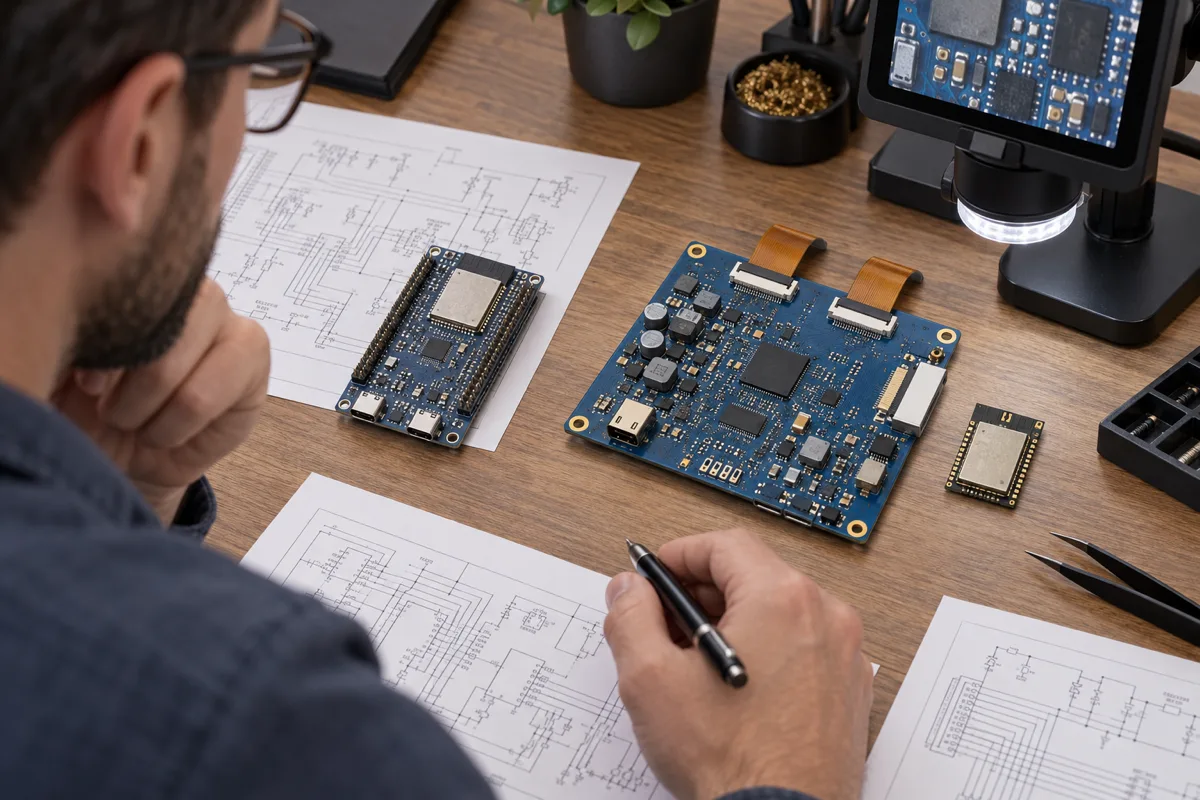
This is an editorial illustration, not a photograph or validation result from a target board.
Espressif's PCB layout guide recommends at least four layers and a continuous reference ground, and gives rules for MIPI differential impedance, intra-pair/inter-pair length, via return paths and separation from other high-speed or high-frequency signals and switching-supply interference. Separately, the schematic checklist calls for provision for series resistors on MIPI lines and the prescribed CSI/DSI REXT pulldowns. RF-module coexistence on the target board still needs its own review and test; the layout guide is not a completed antenna-clearance qualification. Hardware, mechanical and firmware engineers need one interface table covering board traces, connector, FPC and receiving device. Perfect board-length matching cannot rescue a reversed FPC pinout or wrong sensor control voltage.
If the product does not use MIPI, the official rules may allow the associated supply and external-resistor pins to remain unconnected. Do not fan out a dormant high-speed interface to an unexamined “future” connector: it still consumes layers, space and signal-integrity margin. Conversely, if camera and display must run together, successful enumeration of both interfaces does not establish throughput. Test the target board at the actual resolution and network load while recording buffer use, DMA behavior, sustained heat and visible stability. No target-board measurements are available for this article, so it makes no frame-rate promise.
Establish the physical link before tuning performance
For a camera with no frames, capture sensor power, reset, clock and I2C identification before chasing CSI lanes and pixel formats. For a black screen, check panel power, reset, initialization commands, backlight and DSI lane assignment. Tuning ISP, PPA or LVGL before those checks can misclassify a physical-link fault as a software-performance problem.
Once the basic links work, document three separate operating conditions: static image, sustained frames, and camera/display/wireless concurrency. Record each condition's input, error counts and memory high-water mark. A comparison between EV Board and product board is meaningful only within the same condition, matching sensor, panel, firmware, load and capture window and naming any unavoidable board-level difference. Do not subtract the results of unlike workloads and call the delta a board improvement.
Treat the FPC as a versioned, replaceable component. Length, shielding, contact orientation and assembly tolerance can change a high-speed path; production may install a visually similar reverse-contact cable. Sample records should include its part number, length and assembly orientation. If the screen or camera is serviceable, carry those facts into incoming inspection and repair instructions as well.
Wireless and recovery are board-design decisions
P4 has no integrated Wi-Fi. Following the EV Board's C6 pattern means the product PCB must provide C6 power, antenna clearance, an inter-chip bus and independent reset/programming access. In ESP-Hosted, control RPCs and data frames cross that bus; transport configuration and firmware versions at both ends have to be compatible. A networking demo on the EV Board says nothing about a new enclosure's antenna, custom inter-chip routing or a companion that becomes unresponsive.
This is not another tutorial on the P4+C6 software stack. It is a hardware-review demand: can P4 boot and report a fault when C6 does not answer? Can a jig identify and reflash both chips separately? Can antenna placement coexist with MIPI routing? Is RF and thermal behavior still acceptable with the enclosure closed? Assign owners and test methods for those questions before board release, rather than asking field firmware engineers to improvise recovery after shipment.
Provide an explicit manufacturing and repair route. P4 and C6 images may have separate versioning, signing, update and rollback requirements. A P4-only debug header cannot recover a bricked C6 without disassembly. Expose accessible test points for both devices, external Flash and important rails, and record both image identities and a basic handshake result. Pin selection, jig and test duration depend on the actual board; “we reserved pads” is not equivalent to a power-cut and failed-flash recovery exercise.
Diagnose three different kinds of offline device
First, P4 itself may fail to boot: recovery must work without a screen or network. Second, P4 may run while C6 does not handshake: identify C6 supply, reset and firmware before declaring the whole product healthy. Third, both chips may boot but Wi-Fi remain unreliable: only then investigate antenna, enclosure, access point and data path. Give each case a minimum observable signal and a minimum recovery action so that technicians do not reflexively reflash P4 for every offline report.
Firmware release scope must include hardware combinations. If a product ships with different silicon revisions, panels or wireless modules, an application version alone cannot describe compatibility. Keep a readable BOM/hardware identity and a firmware compatibility map. This is not a call to build a broad fleet-management platform on day one; it prevents a known-incompatible image being sent to a visually identical device. Verify the selected SDK's partitioning, signing and rollback capabilities on the actual board before promising them.
Four reviews turn a reference design into your own
1. Freeze requirements. Name the production panel, sensor, wireless module, USB interface, storage and enclosure, and list every EV Board component to be replaced. 2. Review the schematic. For the chosen chip revision and errata, check power, clocks, reset, Flash, voltage domains, MIPI control pins and debug access, each with an official reference and owner. 3. Review PCB and assembly. Check stack-up, impedance, return path, pair matching, FPC orientation, antenna placement and hot spots. 4. Verify the target board. Save both firmware identities and boot logs, then run reproducible display/camera/network concurrent loads, power disturbance, interrupted update and repair exercises.
After the first two reviews you can say the design has a documented basis. After the third, drawings and layout have been reviewed. Only target-board records from the fourth support a claim that a specified sample worked under specified conditions. Production readiness also needs pilot yield, batch consistency and the compliance process for the intended markets. Until those records exist, the honest conclusion is “a custom-board design ready for verification,” not “the EV Board has been converted into a qualified production design.”